What data recovery tools to buy if you want to start a data recovery business?
Free video data recovery training on how to recover lost data from different hard drives?
Where to buy head and platter replacement tools at good prices?
Data recover case studies step by step guide
I want to attend professional data recovery training courses
If you’re going to replace the chip of your flash drives for repairing purpose or for upgrading your flash drives with a larger capacity, the following information can be useful to you.
Firstly you need to find a donor chip. You can find these chips by purchase from some trusted memory chips suppliers or from some dead donor flash drives.
This forum post can be useful to get the donor chip!
How to extract the flash chip from a donor?
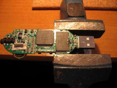
The following example is based on a A donor s1mp3, it had the same flash memory chip of the target, a 4Gbit Samsung.
Open the donor and secure it to a table.
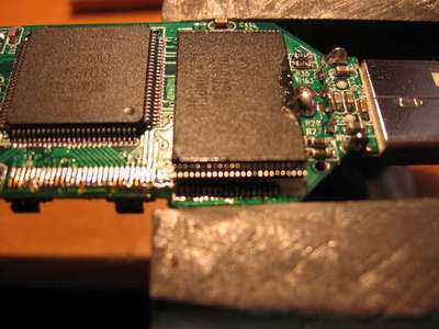
Put up one side of chip and gently apply some heat to desolder it. Besides, you can use a sharp, thin razor blade to cut the pins off. Hold the blade as closely to the board as possible, this keeps the pins long enough for soldering.
- Do not overheat chip with soldering gun/iron.
- Do not cut chip legs. Almost all of them are necessary
Then, take the same operation with the other side. Now you can extract the memory chip from the donor.
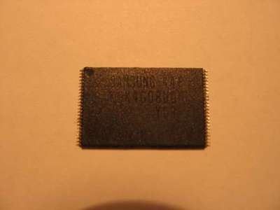
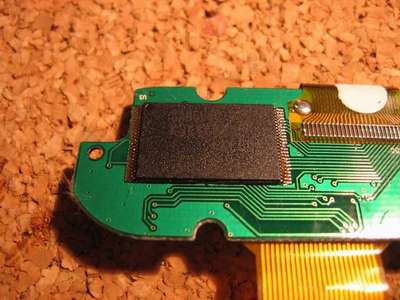
Here’s the 4Gbit flash chip. Pins will be dirty after removal (tin + rosin). Clean it so there are no short circuits. It is now ready to use!
Now, let’s solder the second chip
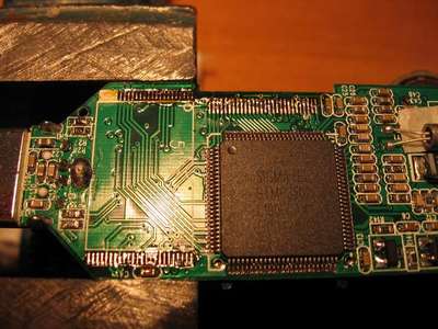
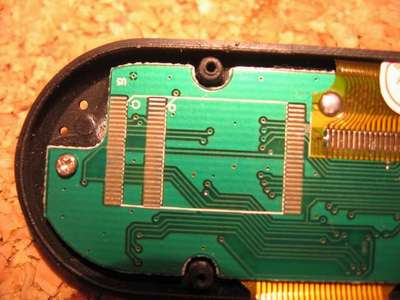
Open the target s1mp3 and secure it to a table, with the free soldering place face up.
The “o” symbol marks position of first pin of memory chip! This is very important! You can’t turn chip around during soldering. The chip MUST be correctly aligned! Take a look at the pin 1 marker embossed on the chip.
Clean the free soldering place on the circuit board of the target S1mp3 with alcohol, if necessary.
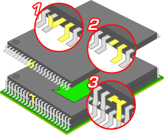
If your board does not have the soldering points for another memory chip, you can still add a second chip following this scheme:
NOTE: This piggy-backing method will not allow you to have a player with more than two memory chips! It relies on the fact that both chip enable lines are brought out on pins 9 and 10 of the first memory chip socket/solder pads. So, solder all the pins of the second memory at the top of the first, making the addaptation on the legs 9-10.
Soldering the chip
Apply tin to solder the chip legs to the board. This is the most dangerous and difficult part as the pins are so small and close that it is very easy for solder to bridge across the pins.
Tips:
- Use as little tin as possible. Soldering areas are just covered – it should be enough.
- Put the chip very precisely on the soldering places.
- Solder first and last pin, then check if location of chip is correct. If it’s OK, then solder the rest of the pins – side by side.
- STOP and CHECK with multimeter and magnifying glass (or grandma’s “+4” glasses), MAKE SURE that there are no short-circuits between chip legs.
Sometimes flash chip’s include two chips in one case. E.g. a 1GB chip could contain 2x 512MB chips. Then the chips second enable signal (CE2) also needs to get connected. The boards usually keep this pin unconnected/floating. This causes the whole bus to break down. Either remove the old chip’s CE line and connect to this pin (CE1) or directly connect to VCC and waste the memory. Another option may be to add a switch.
Reference: s1mp3.org wiki
Data recovery salon is always sharing the best and smart information with all and we welcome public comments and ideas to improve Data recovery salon together and then we make progress together!



1 Comment
if you like i can reword the bit you added as i understand it:
The reason why the piggybacking works is Sometimes flash ICs include two chips in one case. E.g. a 1GB IC could contain 2x 512MB chips. if the board is designed for dual chips then the piggyback IC can connect to the second enable (ce2) as shown, but if the board is not designed for this, Then the piggyback IC enable signal still needs to get connected. The boards designed for one chip/IC usually keep this pin unconnected/floating. This causes the whole bus to break down because chips in either IC are enabled at once, NC=enabled. Either remove the old IC’s CE line(s) and connect its CE pins to VCC to disable the chip. Another option may be to add a switch.